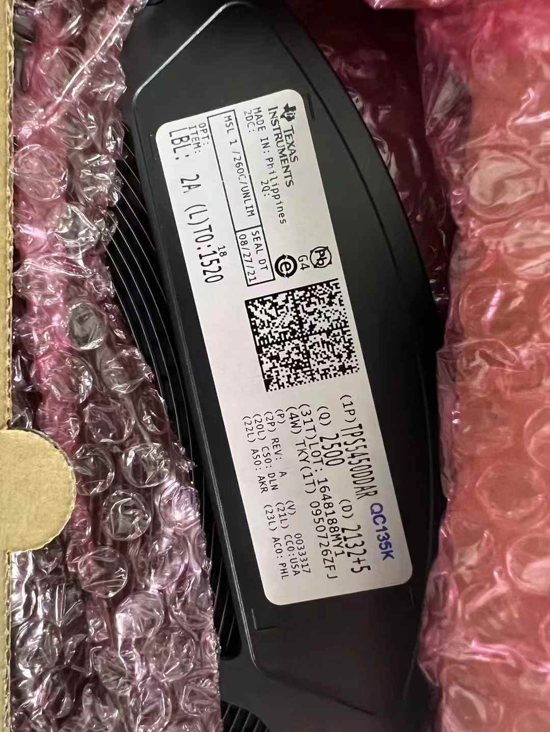
The TPS5450 is a high-output-current PWM converter that integrates a low-resistance, high-side N-channel MOSFET. Included on the substrate with the listed features are a high-performance voltage error amplifier that provides tight voltage regulation accuracy under transient conditions; an undervoltage-lockout circuit to prevent start-up until the input voltage reaches 5.5 V; an internally set slow-start circuit to limit inrush currents; and a voltage feed-forward circuit to improve the transient response. Using the ENA pin, shutdown supply current is reduced to 18 μA typically. Other features include an active-high enable, overcurrent limiting, overvoltage protection and thermal shutdown. To reduce design complexity and external component count, the TPS5450 feedback loop is internally compensated.
The TPS5450 device is available in a thermally-enhanced, 8-pin SOIC PowerPAD package. TI provides evaluation modules and software tool to aid in achieving high-performance power supply designs to meet aggressive equipment development cycles.
德克萨斯仪器tps5450ddar
是的tps5450高输出电流PWM转换器,集成了低电阻、高侧N沟道MOSFET。包括与上市特点基材是一种高性能的电压误差放大器,提供了严密的电压调节精度瞬态条件下;欠压锁定电路防止启动至输入电压达到5.5 V;内部设置一个慢启动电路限制浪涌电流;和电压前馈电路来提高系统的暂态响应。使用ENA引脚关断电源电流降低到18μ典型。其他功能包括一个积极的高启用,过流限制,过压保护和热关机。为了减少设计的复杂性和外部元件,该tps5450反馈回路是内部补偿。
的tps5450装置在热增强可用,8引脚SOIC PowerPad封装。TI提供评估模块和软件工具,以帮助实现高性能电源设计,以满足积极的设备开发周期。


 | 0 orders
 -->Arrival time 5-7 days
 ---->Arrival time 15-27 days
 -->Arrival time 5-7 days
 Datasheet
