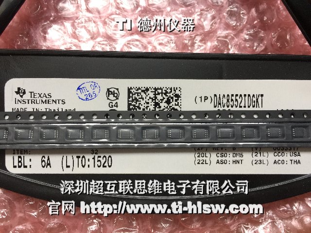
The DAC8552 is a 16-bit, dual channel, voltage output digital-to-analog converter (DAC) offering low power operation and a flexible serial host interface. Each on-chip precision output amplifier allows rail-to-rail output swing to be achieved over the supply range of 2.7V to 5.5V. The device supports a standard 3-wire serial interface capable of operating with input data clock frequencies up to 30MHz for VDD = 5V.
The DAC8552 requires an external reference voltage to set the output range of each DAC channel. Also incorporated into the device is a power-on reset circuit which ensures that the DAC outputs power up at zero-scale and remain there until a valid write takes place. The DAC8552 provides a flexible power-down feature, accessed over the serial interface, that reduces the current consumption of the device to 700nA at 5V.
The low-power consumption of this device in normal operation makes it ideally suited for portable, battery-operated equipment and other low-power applications. The power consumption is 0.5mW per channel at 2.7V, reducing to 1µW in power-down mode.
The DAC8552 is available in a MSOP-8 package with a specified operating temperature range of -40°C to +105°C.


 | 0 orders
 -->Arrival time 5-7 days
 ---->Arrival time 15-27 days
 -->Arrival time 5-7 days
 Datasheet
